AXI Bus
AXI4 Protocol
A detour to learn the interface generation phase of HLS (Adapt to Xilinx FPGA)
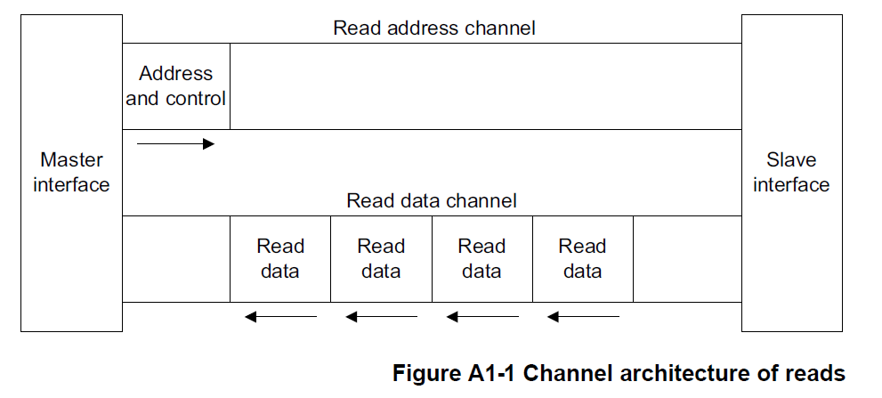
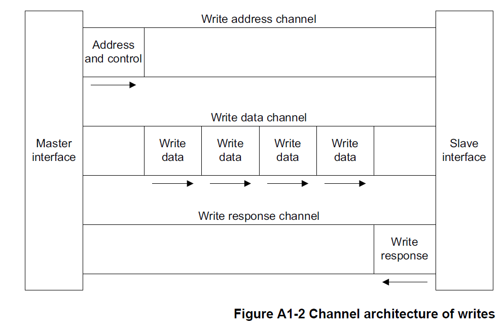
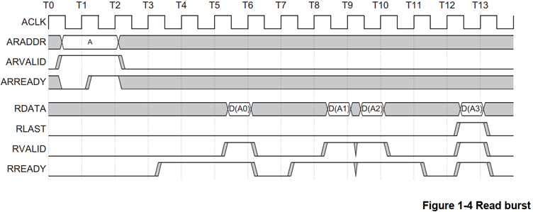
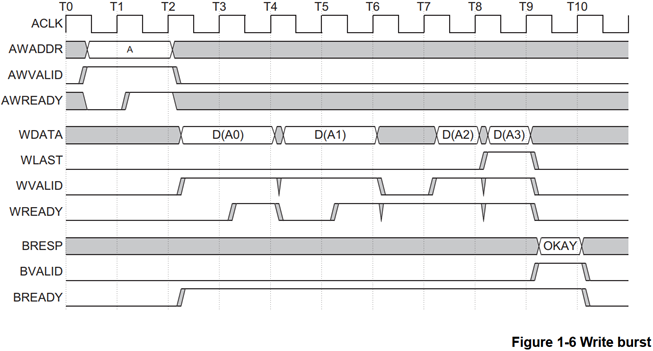
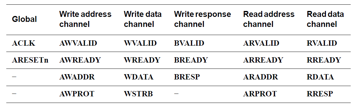
The AXI protocol is burst-based and defines the following independent transaction channels
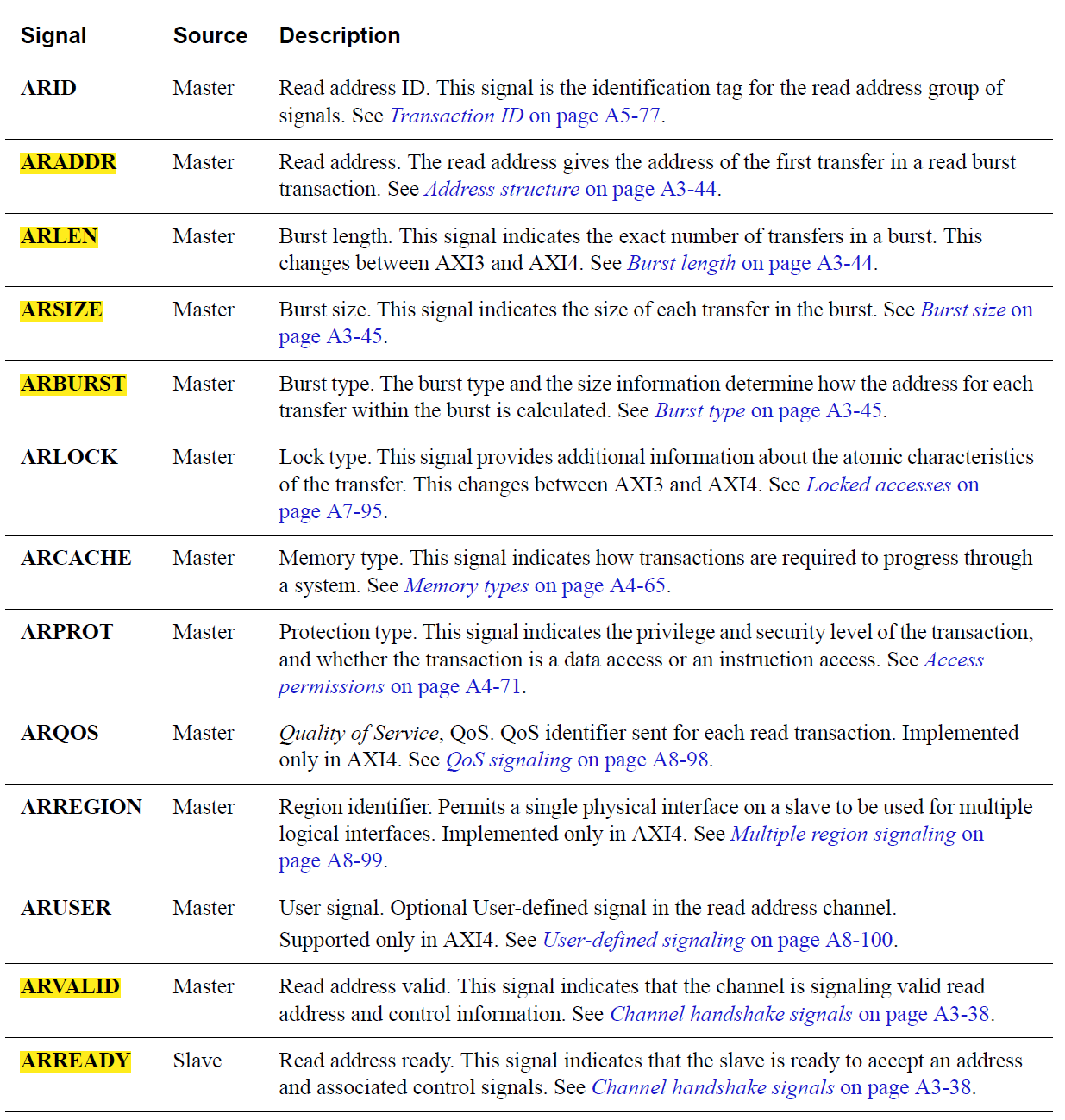
- read address
- read data
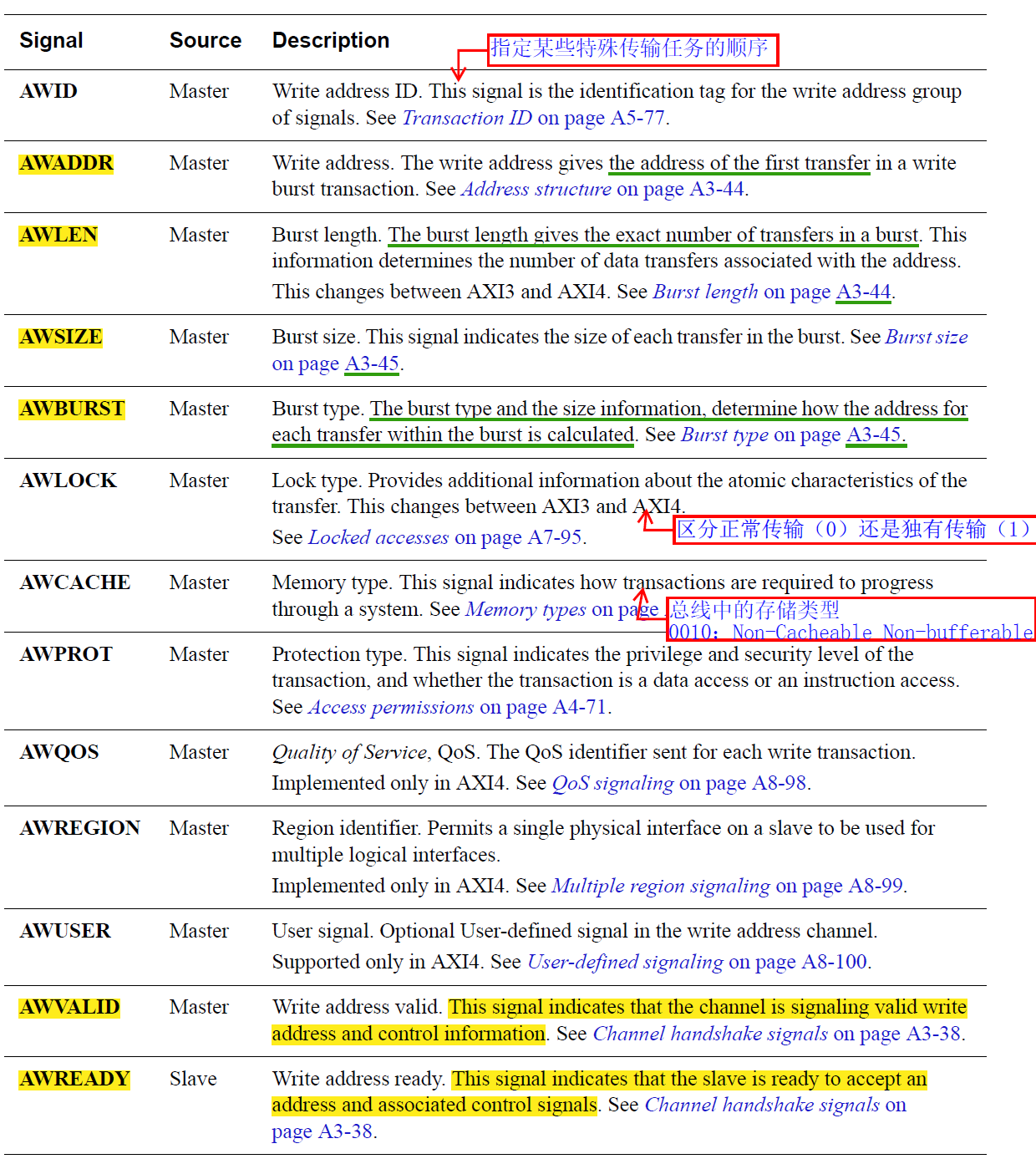
- write address
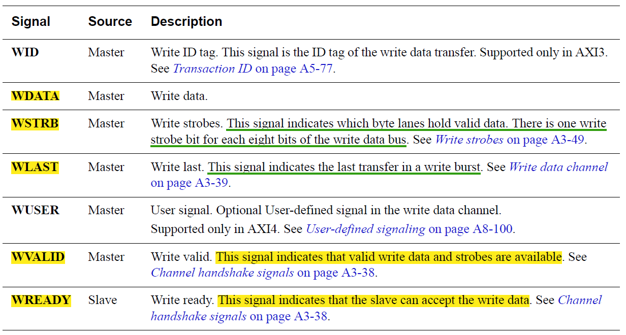
- write data
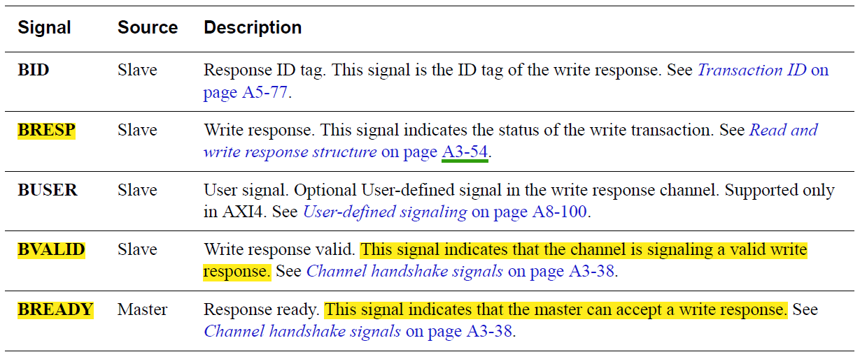
- write response.
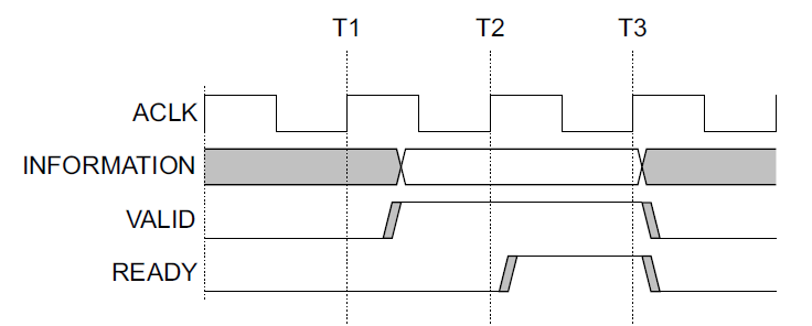
Each of the independent channels consists of a set of information signals and VALID and READY signals that provide a two-way handshake mechanism. The information source uses the VALID signal to show when valid address, data or control information is availableon the channel. The destination uses the READY signal to show when it can accept the information. Both the readdata channel and the write data channel also include a LAST signal to indicate the transfer of the final data item in a transaction
Handshake Process
All five transaction channels use the same VALID/READY handshake process to transfer address, data, and control information.
- The source generates the VALID signal to indicate when the address, data or control information is available.
- The destination generates the READY signal to indicate that it can accept the information.
- Transfer occurs only when both the VALID and READY signals are HIGH.
Signal Descriptions
Global Signals
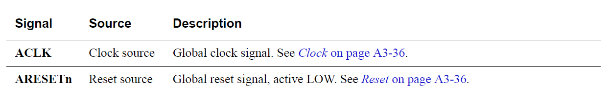
- CLK: All signals are sampled on the rising edge of the global clock. Each AXI component uses a single clock signal, ACLK. All input signals are sampled on the rising edge of ACLK. All output signal changes must occur after the rising edge of ACLK.
- RST: The AXI protocol uses a single active LOW reset signal, ARESETn. The reset signal can be asserted asynchronously.During reset the following interface requirements apply: a master interface must drive ARVALID, AWVALID, and WVALID LOW; a slave interface must drive RVALID and BVALID LOW.
Write address channel signals
Write data channel signals
Write response channel signals
Read address channel signals
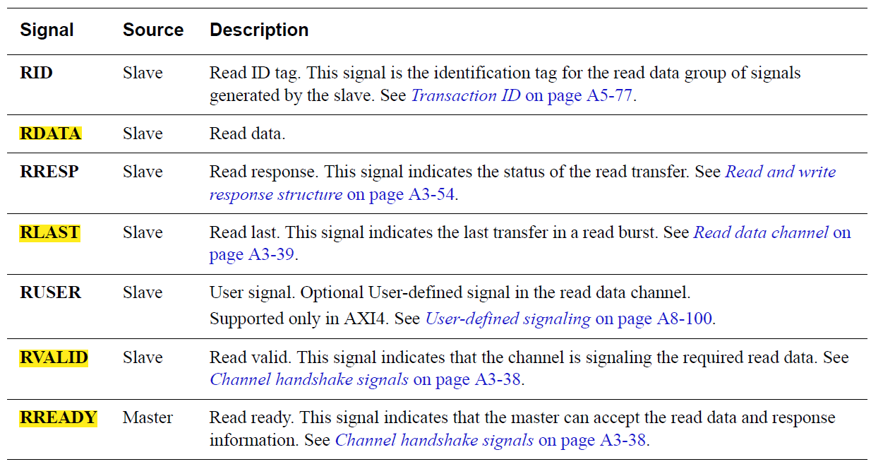
Read data channel signals
Burst W/R
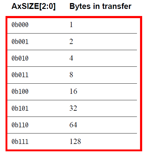
Burst_Length = AxLEN[7:0] + 1The maximum number of bytes to transfer in each data transfer, or beat, in a burst, is specified by ARSIZE[2:0], for read transfers, AWSIZE[2:0], for write transfers
AXI-Lite
The key functionality of AXI4-Lite operation is:
- all transactions are of burst length 1
- all data accesses use the full width of the data bus AXI4-Lite supports a data bus width of 32-bit or 64-bit.
- all accesses are Non-modifiable, Non-bufferable
- Exclusive accesses are not supported.
Xilinx M-AXI Adapter (Burst transaction)
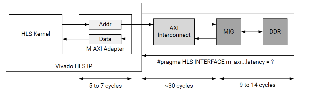
When your design makes a read/write request, the request is sent to the DDR through several specialized helper modules. First, the M-AXI adapter serves as a buffer for the requests created by the HLS kernel. The adapter contains logic to cut large bursts into smaller ones (which it needs to do to prevent hogging the channel or if the request crosses the 4 KB boundary, see Vivado Design Suite: AXI Reference Guide (UG1037)), and can also stall the sending of burst requests (depending on the maximum outstanding requests parameter) so that it can safely buffer the entirety of the data for each kernel. This can slightly increase write latency but can resolve deadlock due to concurrent requests (read or write) on the memory subsystem.